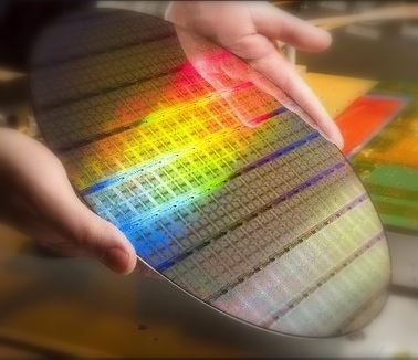
The following notes examine just a few of the Atmospheric Plasma Applications for Semiconductors, IC and Electronics Assembly that Intrface Technologies has worked with. We have utilized our atmospheric plasma technology in applications such as wafer to wafer bonding, indium tin oxide deposition, flex circuits, lead free soldering, lead frame and critical device and component packaging requirement.
 Vacuum plasma technologies are well characterized in the semiconductor processing and electronics assembly industries. Atmospheric plasma technology is relatively new to the field and allows for lower cost of entry and operation as well as high speed in-line processing. The automobile electronics industry is utilizing atmospheric plasma for advancing reliability in the ever increasing amount of electronics, computers, batteries, components, assemblies and touch screens being utilized in modern vehicles.
Glass and polymer cleaning and activation with atmospheric plasma is commonly performed prior to thin film coatings or bonding cover glass in applications such as smartphones and other touch screen protective coverings of Corning® Gorilla® Glass or sapphire.
Related articles:
- Cada, M., Churpita ,O., Hubicka, Z., Sichova, H., and Jastrabik, L., “Investigation of the low temperature atmospheric plasma deposition of TCO thin films on polymer substrates,” Surf. Coat. Technol. 177, 699 (2004). Abstract: Atmospheric barrier–torch discharge was used for low temperature deposition of thin conductive oxide thin films on polymer substrates. An atmospheric high-density plasma jet was excited at the outlet of the quartz nozzle with an external metallic ring electrode. The RF power was capacitively connected to the plasma via a dielectric wall of the quartz tube. There was not a direct contact of the atmospheric plasma with the metallic electrode in this configuration. InxOy and SnOx transparent and conductive thin films were deposited on polymer, quartz and silicon substrates by this technique. Vapours of solid phase of In-acetylacetonate and Sn-acetylacetonate carried by nitrogen flow were used for deposition of InxOy and SnOx thin films, respectively and vapours prepared of liquid solutions of In3-tetramethylheptanedionate in n-Oktan. Some atmospheric plasma jet parameters were determined by emission spectroscopy and by planar Langmuir probe. Deposited films were analysed by means of electron microprobe system, XRD diffraction and electrical conductivity measurement.
- Kwang-Seok Kim, Woo-Ram Myung and Seung-Boo Jung., “Effects of Plasma Polymerized Acrylic Acid Film on the Adhesion of Ag Tracks Screen-Printed on Polyimide,” The Journal of Adhesion, 88:1–13, 2012. Abstract: The adhesion of conductive patterns printed on polymer substrates is an indispensible issue for the commercialization of printable and flexible electronic devices. Plasma treatment has been widely used to improve the interfacial adhesion between a metal and a flexible polymer substrate. This study aims to investigate the influence of a polymerized acrylic acid layer coated by atmospheric-pressure plasma (APP) on the adhesion of a screen-printed silver (Ag)/polyimide (PI) system. The acidic oxygen-containing functional groups were incorporated onto a PI film by plasma polymerization of acrylic acid and, on it, the conductive tracks were constructed with a Ag nanopaste via screen printing. The Ag tracks were sintered at various temperatures ranging from 150 to 300°C for 30 min in air. The adhesion was evaluated by a roll-type 90% peel test. The peel strength of the screen-printed Ag/PI system with the acrylic acid film approximately quadrupled. To understand this adhesion enhancement, field emission scanning microscopy (FE-SEM), atomic force microscopy (AFM), contact angle analyzer, and X-ray photoelectron spectroscopy (XPS) were utilized. It was confirmed from these analyses that a hydrophilic film was formed due to the plasma polymerization process, and the carbon-oxygen (C–0)and carbonyl (C=0) bonds increased at the interfacial surface. Under the optimized conditions, a maximum adhesion of 245.5 N/m was obtained, and the stronger adhesion with the acrylic acid coating influenced the improvement in the flexibility of the film.
- Habib, S. B., Gonzalez, E., and Hicks, R. F., “Atmospheric oxygen plasma activation of silicon (100) surfaces,” J. Vac. Sci. Technol. A, submitted August 14 (2009). Abstract: Silicon (100) surfaces were converted to a hydrophilic state with a water contact angle of <5° by treatment with a radio frequency, atmospheric pressure helium, and oxygen plasma. A 2 in. wide plasma beam, operating at 250 W, 1.0 l/min O2, 30 l/min He, and a source-to-sample distance of 3±0.1 mm, was scanned over the sample at 100±2 mm/s. Plasmaoxidation of HF-etched silicon caused the dispersive component of the surface energy to decrease from 55.1 to 25.8 dyn/cm, whereas the polar component of the surface energy increased from 0.3 to 42.1 dyn/cm. X-ray photoelectron spectroscopy revealed that the treatment generated a monolayer of covalently bonded oxygen on the Si(100) surface0.15±0.10 nm thick. The surface oxidation kinetics have been measured by monitoring the change in water contact angle with treatment time, and are consistent with a process that is limited by the mass transfer of ground-state oxygen atoms to the silicon surface.
Contact us to find out more about Atmospheric Plasma Applications for Semiconductors, IC and Electronics Assembly or to receive a complimentary copy of the technical articles above utilizing atmospheric plasma. Please reference the authors and publication number in your email request (copy and paste into your email response).